
PDK Fill runset development engineer
Job Description
? Designs, develops, tests, and debugs software tools, flows, PDK design components, and/or methodologies used in design automation and by teams in the design of hardware products, process design, or manufacturing. ? Responsibilities include capturing user stories/requirements, writing both functional and test code, automating build and deployment, and/or performing unit, integration, and end to end testing of the software tools. ? In this position the candidate is expected to be well versed in Calibre or ICV or Pegasus verification languages and can provide algorithmic solutions to meet manufacturing needs. The ideal candidate will have the following skills: ? Candidate also expected to grow talent and have good communication, verbal, and written skills.Qualifications
Minimum Qualifications: ? Bachelor in Electrical Engineering/Computer Engineering with 12+ years of semiconductor industry experience or Masters degree with 10+ years of experience OR ? PhD in Electrical Engineering, Computer Engineering with the proven experience of 8+ years in the semiconductor industry. Experience in the following areas: ? Rule deck/runset development using Calibre (svrf) or ICV (rs) or Pegasus (pvl) with exposure to VLSI design and execution. ? Algorithmic development and translating rules into runsets. ? Automation using Python, and Unix-Linux platforms. ? Developing test cases to validate DRC, LVS, antenna, density and fill modules. Preferred Qualifications: ? Exposure to multiple EDA verification languages is a plus (Synopsys ICV, Cadence Pegasus, Siemens Calibre) ? Exposure to layout, schematic entry using Cadence Virtuoso and Synopsys Custom Designer ? Exposure to semiconductor device physics models and technology scaling ? Familiar with industry standard CAD tools flows for digital analog designInside this Business Group
As the world's largest chip manufacturer, Intel strives to make every facet of semiconductor manufacturing state-of-the-art -- from semiconductor process development and manufacturing, through yield improvement to packaging, final test and optimization, and world class Supply Chain and facilities support. Employees in the Technology Development and Manufacturing Group are part of a worldwide network of design, development, manufacturing, and assembly/test facilities, all focused on utilizing the power of Moore’s Law to bring smart, connected devices to every person on Earth.Posting Statement
All qualified applicants will receive consideration for employment without regard to race, color, religion, religious creed, sex, national origin, ancestry, age, physical or mental disability, medical condition, genetic information, military and veteran status, marital status, pregnancy, gender, gender expression, gender identity, sexual orientation, or any other characteristic protected by local law, regulation, or ordinance.Benefits
We offer a total compensation package that ranks among the best in the industry. It consists of competitive pay, stock, bonuses, as well as, benefit programs which include health, retirement, and vacation. Find more information about all of our Amazing Benefits here.It has come to our notice that some people have received fake job interview letters ostensibly issued by Intel, inviting them to attend interviews in Intel’s offices for various positions and further requiring them to deposit money to be eligible for the interviews. We wish to bring to your notice that these letters are not issued by Intel or any of its authorized representatives. Hiring at Intel is based purely on merit and Intel does not ask or require candidates to deposit any money. We would urge people interested in working for Intel, to apply directly at https://jobs.intel.com/ and not fall prey to unscrupulous elements.Working Model
This role will be eligible for our hybrid work model which allows employees to split their time between working on-site at their assigned Intel site and off-site. In certain circumstances the work model may change to accommodate business needs.
Maggie Offensive Security Researcher
“I’ve always wanted to do something that changes the world — at Intel, I feel appreciated, and I’ve gained more confidence in myself. It makes me feel like I’m capable of doing great things.”
- Solutions and Services Category Planning and Launch, NEX Sales Santa Clara, California View job
- Software Application Development Engineer Guadalajara, Mexico View job
- Custom Design Reference Flow Engineer Bengaluru, India View job
You don't have Saved Jobs yet.
View all jobs-

-
-
-
-
-
-
-
-
-
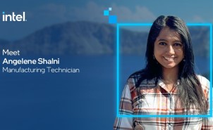
Angelene Shalni: A Medical Enthusiast's Tech Transformation
Meet Angelene Shalni Kumarasan who transitioned from a medical aspirant to a Manufacturing Technician, triumphing over stereotypes. She now leads Intel's Pelican Project while studying electrical engineering.
-
Perks & Benefits
Your total rewards package also includes health and wellness and retirement benefits. We provide the support you need to thrive.
-
Interns and Grads
Ready to start more than just your career? This could be the beginning of something amazing.
-
Life at Intel
We've created an inclusive, supported environment...and we can't wait for you to be a part of it.
-
Our Software Teams
Intel is one of the largest and most influential software companies in the world. See software jobs for developers and engineers at Intel.
-
Location: Germany
We have offices in Munich and Karlsruhe, and we are building a new fab in Magdeburg. Discover what it's like to work at Intel Germany.
-
-
-
Location Spotlight: Ireland
Discover how it's to work with us. See Intel jobs in Ireland.
-
Location Spotlight: Ohio
Discover how it's to work with us. See Intel jobs in Ohio.
-
Location Spotlight: Hillsboro
Discover how it's to work with us. See Intel jobs in Oregon.
-
Intro to Semiconductors
Semiconductors—otherwise known as microchips, microprocessors, or chips—are the brains behind some of the most innovative technology today. Learn more about our plans for innovation and growth—and why your career should start with Intel.
-
-
-
Location Spotlight: Folsom
Discover how it's to work with us. See Intel jobs in Folsom.
-
Hear from Our People: Ireland
From engineers and scientists to manufacturing technicians and number crunchers, all our people share a great ambition and an anything-is-possible attitude to create, innovate, and improve the world around us.
-
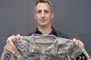
Veterans
We connect the best and brightest military talent to Intel careers where you can continue to make an impact and build the future.
-
Location Spotlight: Chandler
Discover how it's to work with us. See Intel jobs in Chandler.
-
Women in Tech | Intel Careers
As a woman in tech, you’re a disruptor and a change agent. Start your next chapter with Intel.
-
-
Ireland: The Intel Insider Podcast
Stories from the people behind the tech Get inside life at Intel Ireland. Host Anna Geary chats to the people of Intel about their career, their work, and their life at one of the world's most established tech companies.
-
Finance Intern Alexis Crowell's Rise to Tech Visionary
Discover Alexis Crowell's journey from a finance intern to VP and GM of Intel’s SMG in APJ, leading diverse teams, spearheading integral programs, and making significant strides in AI and machine learning.
-
Dr. Beth Yam: Pioneering Malaysia's Manufacturing Sector
From a fresh graduate to Intel Malaysia's first female principal engineer, Dr. Beth Yam's journey is nothing short of inspiring. Currently, she heads the Penang Disaggregation Manufacturing and continues to make her mark.
-
AI Leadership: The Remarkable Journey of Srinivas Lingam
Srinivas Lingam, now VP, AI Acceleration Office & GM, Habana Labs India, has transitioned from a college geek to a respected industry veteran, contributing significantly to Intel's tech leadership.
-
College Graduate Careers at Intel India
Follow the careers of Raj and Ankita who describe both their internship and early career experiences at Intel.
-
Meet Martin, SoC Design Engineer and Former Intern
Martin shares his experience of converting from an intern to a full-time employee.
-
Our Hiring Process
See all the steps of the recruitment process at Intel – from apply to interview.
-
Interview Tips
Prepare for your interview at Intel using the resources, practice questions, tips and tricks we’ll provide here!
-
AfroTech
We value diverse perspectives and we're dedicated to creating a responsible, inclusive, and sustainable world through technology.
-
Diversity & Inclusion
See how we're ensuring that inclusivity and accountability are embedded in our culture globally.
-
Global Impact (RISE)
Learn about our strategy and goals for a more responsible, inclusive, and sustainable world, enabled through technology and our collective actions.
-
Location Spotlight: Austin
Discover how it's to work with us. See Intel jobs in Austin.
-
Location Spotlight: Atlanta
Discover how it's to work with us. See Intel jobs in Atlanta.
-
Our AI Teams
Apply your skill in advancing Artificial Intelligence to create solutions that will change the world. See AI and machine learning jobs at Intel.
-
Our Corporate Functions Teams
Your role as a business professional at Intel will help us forge success with our products, finances, and people. See HR, finance, and other corporate jobs at Intel.
-
Our Hardware Teams
Intel is a leading hardware company. See our job offers for hardware engineers: microprocessor jobs, PCB design or platform engineering jobs at Intel.
-
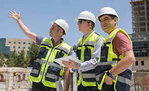
Our Construction & Facilities Teams
Build Intel’s manufacturing sites’ infrastructure and develop strategies for complex projects. See facilities management and fab jobs at Intel.
-
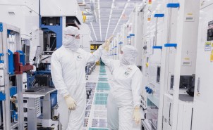
Our Manufacturing & Process Development Teams
Our manufacturing and process development specialists build some of the best processors in the world. See factory, technician and process engineer jobs at Intel.
-
Our Sales & Marketing Teams
Our Sales and Marketing team manage strong, long-term relationships with partners to solve business problems. See sales and marketing jobs at Intel.
-
Our Silicon Photonics Teams
Explore some of the most exciting applications of light-based data transfer among computer chips. See semiconductor and silicon jobs at Intel.
-
Our Information Technology Teams
Join one of the best tech companies. Intel's IT team is looking for information technology engineers, support technicians, security specialists, and IT help desk support.
-
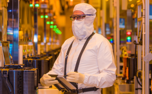
Manufacturing Technicians | Intel Careers
Our Manufacturing Technicians are critical to Intel and the future of technology. See manufacturing careers.
-
Location Spotlight: Rio Rancho
Discover how it's to work with us. See Intel jobs in New Mexico.
-
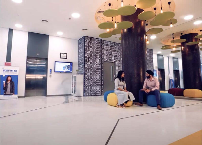
Location Spotlight: India
Discover how it's to work with us. See Intel jobs in India.
-
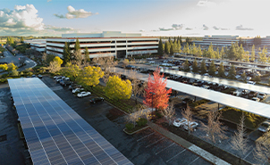
Location Spotlight: Santa Clara
Discover how it's to work with us. See Intel jobs in Santa Clara.
-
#Intern4Intel
This is the story of three women who started their careers as interns with Intel and are now full-time employees--listen to their journey!
-
Intel in Romania
Discover how it is to work with us. See jobs in Romania.
-
Location Spotlight: Fort Collins
Discover how it's to work with us. See Intel jobs in Colorado.
-
Strength in Flexibility
Jennifer explains how the flexibility she has at Intel allows her to balance her career with caring for her daughter, Nora, who has a rare genetic disorder.
-
Location: Poland, Wroclaw
Learn more about Intel's Assembly and Test Facility in Poland, Wroclaw. Check out what kind of manufacturing jobs we are opening.
-
-
Intel Foundry | Intel Careers
Intel Foundry is an independent foundry business that meets our customers’ unique product needs. View all foundry careers.
-
-
Data Science and Analytics Teams
Solve real-world challenges, improve processes and use analysis to predict future trends. See data science, data analytics and other data jobs at Intel.
-


Join Our Talent Community
Be the first to hear about what's happening at Intel! Sign up to receive the latest news and updates.