
FSM Global Yield Defect Reduction Senior Development Engineer
Job Description
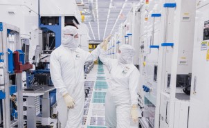
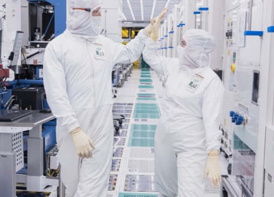
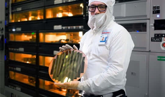
Fab Sort Manufacturing (FSM) is responsible for the production of all Intel silicon using some of the world's most advanced manufacturing processes in fabs in Arizona, Ireland, Israel, Oregon and 2 new greenfield sites in Ohio and Germany. As part of Intel's IDM2.0 strategy, FSM is rapidly expanding its operation to deliver output for both internal and foundry customers with state-of-the-art technologies arriving in High-Volume Manufacturing (HVM) at a 2-year cadence going forward. Intel recently created HVM Global Yield organization in FSM to strengthen its yield operation and enable fast-paced yield ramp-up in early HVM phases for each technology in collaboration with Technology Development team and FSM fab managers.
This job requisition is to seek for Defect Metro Development engineering roles in FSM HVM Global Yield organization, reporting to Defect Metro Engineering Development manager. Selected candidates will work with other members in defect metro team, other teams in Global Yield org, fab module, yield, integration and TD team members to achieve yield ramp-up and defect reduction in early production stage, supporting internal and external customers.
Collaborate with Technology Development team and Process Integration team to import and setup new technology to production fabs across the globe.
Identify critical yield limiting defect steps and work with Defect Control team to set production line inspection strategy to protect yield and quality at maximum productivity and lowest cost.
Candidate should possess the following behavioural skills:
- Problem-solving and project/program management experience with strong self-initiative and self-learning capabilities.
- Demonstrated interpersonal skills to perform at leadership role including influencing, engaging, and motivating.
- Proven track record of working across organization through matrix structures to accomplish strategic objectives with conflicting priorities.
- Must demonstrate strong communication skills.
Qualifications
Minimum qualifications are required to be initially considered for this position. Preferred qualifications are in addition to the minimum requirements and are considered a plus factor in identifying top candidates.
Minimum Qualifications:
- Bachelor’s degree in science and engineering major, with at least 15-18 years of experience.
- Strong understanding on defect mechanism and yield impact in semiconductor high-volume production and proven quantified track record of driving down D0.
- 8+ years of experience in advanced node semiconductor industry in Defect engineering.
- Basic understanding and collaboration experience with processes including lithography, dry etch, wet etch, CMP, diffusion, implant, thin films and metrology.
- Experience in Statistics and Machine Learning preferred.
- Experience in working with Process Integration, Design and OPC teams to identify layout-sensitive defect weak points and address systematic defect issues.
- Knowledge of module tool impacts to defects, inline parametric and yield through PM life while understanding upstream and downstream impacts to other tools
- Experience in FinFET technology development or high-volume manufacturing with hands-on knowledge of FinFET technology process flow to analyse systematic defect sources and set mitigation actions.
- Working knowledge in module processes including lithography, dry etch, wet etch, CMP, diffusion, implant, thin films and metrology. Skills to develop improvement projects at module level to improve process for reduced defectivity and improved yield.
Preferred Qualifications:
- Advanced degree (Master’s or Ph.D.) in Electrical Engineering, Physics, Chemistry or Materials Science major is preferred, with at least 12-15 years of experience.
- Experience in project/program management and/or Task Force Team lead.
- Must demonstrate solid communication skills.
- Ability to work with multi-functional, multi-cultural teams.
- Demonstrated interpersonal skills including influencing, engaging, and motivating.
- Problem-solving technique with strong self-initiative and self-learning capabilities.
- Ability to leverage big data analysis to identify process design weaknesses and/or manufacturing weaknesses to propose corrective, data-based solutions.
- Ability to extracts insights from structured and unstructured data by quickly synthesizing large volumes of data and applying statistics and machine learning.
- Experience in new semiconductor technology development.
- Experience in serving external Foundry customers through technical interactions.
- Experience in GAA (Gate-All-Around) technology architecture.
Inside this Business Group
As the world's largest chip manufacturer, Intel strives to make every facet of semiconductor manufacturing state-of-the-art -- from semiconductor process development and manufacturing, through yield improvement to packaging, final test and optimization, and world class Supply Chain and facilities support. Employees in the Technology Development and Manufacturing Group are part of a worldwide network of design, development, manufacturing, and assembly/test facilities, all focused on utilizing the power of Moore’s Law to bring smart, connected devices to every person on Earth.Posting Statement
All qualified applicants will receive consideration for employment without regard to race, color, religion, religious creed, sex, national origin, ancestry, age, physical or mental disability, medical condition, genetic information, military and veteran status, marital status, pregnancy, gender, gender expression, gender identity, sexual orientation, or any other characteristic protected by local law, regulation, or ordinance.Benefits
We offer a total compensation package that ranks among the best in the industry. It consists of competitive pay, stock, bonuses, as well as, benefit programs which include health, retirement, and vacation. Find more information about all of our Amazing Benefits here.Position of TrustThis role is a Position of Trust. Should you accept this position, you must consent to and pass an extended Background Investigation, which includes (subject to country law), extended education, SEC sanctions, and additional criminal and civil checks. For internals, this investigation may or may not be completed prior to starting the position. For additional questions, please contact your Recruiter.
Maggie Offensive Security Researcher
Ich wollte schon immer etwas tun, das die Welt verändert – bei Intel fühle ich mich geschätzt und ich habe mehr Selbstvertrauen gewonnen. Die Arbeit gibt mir das Gefühl, dass ich in der Lage bin, Großes zu leisten.
- Director, Manufacturing and Sustainability Policy Washington, Washington, D.C. Jetzt bewerben
- Altera BHR Director - EMEA Mehrere Standorte Jetzt bewerben
- Student - Software Development Engineer in Test San José, Costa Rica Jetzt bewerben
Sie haben noch keine gespeicherten Jobs.
Alle Stellenangebote AnsehenSpotlight
-

-
-
-
Vorteile
Umfangreiche bezahlte Freizeit, Aktienoptionen, Weiterbildungsmöglichkeiten, Prämien und vieles mehr. Das ist alles, was Sie brauchen, um erfolgreich zu sein.
-
Praktikanten und Absolventen
Sind Sie bereit, mehr als nur Ihre Karriere zu beginnen? Dies könnte der Beginn von etwas Großartigem sein.
-
Das Leben bei Intel
Wir haben ein einzigartiges Umfeld geschaffen und können es kaum erwarten, dass Sie dazugehören.
-
Intel in Deutschland
Unsere Standorte in München, Karlsruhe und die geplante Megafabrik in Magdeburg bieten eine Vielzahl von Karrieremöglichkeiten. Erkunden Sie Ihre Möglichkeiten!
-
Unser Einstellungsverfahren
Wenn Sie eine Karriere bei Intel anstreben, ist es sinnvoll, sich mit unserem Einstellungsverfahren vertraut zu machen.
-
Das Vorstellungsgespräch
Wir haben für Sie wertvolle Tipps, praktische Ratschläge und hilfreiche Informationen zusammengestellt, damit Sie bei Ihrem Vorstellungsgespräch glänzen können.
-
Our Software Teams
Intel is one of the largest and most influential software companies in the world. See software jobs for developers and engineers at Intel.
-


Werden Sie Mitglied unserer Talent Community
Erfahren Sie immer direkt, was bei Intel passiert! Melden Sie sich an, um die neuesten Nachrichten und Updates zu erhalten.
-
Manufacturing at Intel
Our Manufacturing Technicians are critical to Intel and the future of technology. They are responsible for the setup, maintenance and performance of the complex machinery that build semiconductors—powering nearly everything in our daily lives. Whether you are right out of school, transitioning military, returning to the workforce or looking for a place that values your skills and expertise, we have a place for you at Intel.
-

Life at Intel
We've created an inclusive, supported environment...and we can't wait for you to be a part of it.
-

Learn More About the Semiconductor Industry
Semiconductors—otherwise known as microchips, microprocessors, or chips—are the brains behind some of the most innovative technology today and power so many of the things we use in our daily lives. There’s a big demand for them—and for the talented people who help bring this critical technology to life.
-

Intel to Receive Up to $8.5 Billion Through the CHIPS Act
Proposed funding, coupled with an investment tax credit and eligibility for CHIPS Act loans, would help Intel advance American semiconductor manufacturing and technology leadership in the AI era.
-

Intel Opens Fab 9 in New Mexico
Intel celebrated the opening of Fab 9, its cutting-edge factory in Rio Rancho, New Mexico. The milestone is part of Intel's previously announced $3.5 billion investment to equip its New Mexico operations for the manufacturing of advanced semiconductor packaging technologies.
-
The World’s First Systems Foundry
Intel launched Intel Foundry on February 21, 2024, as a more sustainable systems foundry business designed for the AI era. An expanded process roadmap was announced to establish leadership into the latter part of this decade.


