3D-IC STCO Physical Design Intern.
Job Description
Do Something Wonderful!
Intel put the Silicon in Silicon Valley. No one else is this obsessed with engineering a brighter future. Every day, we create world changing technology that enriches the lives of every person on earth. So, if you have a big idea, let’s do something wonderful together. Join us, because at Intel, we are building a better tomorrow. Want to learn more? Visit our YouTube Channel or the links below!
The Group: Intel's Advanced Design (AD) team resides within the Design Enablement (DE) organization, which collaborates closely with our partners in process technology, IP, and products spanning client/server and networking products. The primary focus of AD is to guide process technology definition, and design prototypes in Intel's latest process technology, supporting Intel's internal and external design customers.
The future of Moore's Law: 3D-IC https://www.intel.com/content/www/us/en/newsroom/opinion/moore-law-now-and-in-the-future.htmlhttps://www.zdnet.com/paid-content/article/moores-law-under-the-microscope-intel-advances-transistor-technology/https://www.tomshardware.com/news/intel-teases-falcon-shores-xpu
The Role:
The Design Technology Pathfinding (DTP) organization in Design Enabling (DE) is chartered to identify and drive key strategic initiatives in the pathfinding of future technologies, as a holistic Design co-optimization across the Product stack from System architecture to silicon as we extend DTCO to STCO (System Technology Co-Optimization). The job requires partnering and leveraging domain experts across Intel and the EDA Eco-System.
Deliverables:
- Run Place and Route to design convergence to establish STCO 2D-3D Physical design baseline, assess quality, perform design analysis and 3D PPA optimization.
- 3D EDA evaluation and methodology development.- Inter chiplet analysis and validation with Synopsys 3D-IC Compiler and Cadence3D Integrity.
- Identify design optimization opportunities (silicon, package, EDA, architecture configuration, methodology, etc)
- Analyze architecture critical paths to identify how to best take advantage of this technology.
- Identify machine learning opportunities for further optimization.
- Highly independent, creative, and out-of-the-box thinker.
This is a fulltime remote or Hybrid (depending on location) internship with a length of 3-4 months, but may be extended to 9+ months.
#DesignEnablement
Qualifications
Minimum qualifications are required to be initially considered for this position. Preferred qualifications are in addition to the minimum requirements and are considered a plus factor in identifying top candidates.
Minimum Qualifications:
Candidate must be actively pursuing a PhD degree in Electrical Engineering or Computer Engineering with 1+ years of experience in the following:
- VLSI and Digital Design.
- Physical Design, Place and Route Tools, Flows, and Methodology.
- Understanding of design methodology .
- Scripting skills using a programming language such Python, TCL or Perl.
Preferred Qualifications:
1+ years of experience in the following:
- Semiconductor Physics.
- Digital and Circuit Design.
- Computer Architecture.
- Machine Learning.
- Logic Design and DFT.
Requirements listed would be obtained through a combination of industry relevant job experience, internship experiences and or schoolwork/classes/research.
Inside this Business Group
As the world's largest chip manufacturer, Intel strives to make every facet of semiconductor manufacturing state-of-the-art -- from semiconductor process development and manufacturing, through yield improvement to packaging, final test and optimization, and world class Supply Chain and facilities support. Employees in the Technology Development and Manufacturing Group are part of a worldwide network of design, development, manufacturing, and assembly/test facilities, all focused on utilizing the power of Moore’s Law to bring smart, connected devices to every person on Earth.Other Locations
US, OR, Hillsboro; US, CA, Santa ClaraPosting Statement
All qualified applicants will receive consideration for employment without regard to race, color, religion, religious creed, sex, national origin, ancestry, age, physical or mental disability, medical condition, genetic information, military and veteran status, marital status, pregnancy, gender, gender expression, gender identity, sexual orientation, or any other characteristic protected by local law, regulation, or ordinance.Benefits
We offer a total compensation package that ranks among the best in the industry. It consists of competitive pay, stock, bonuses, as well as, benefit programs which include health, retirement, and vacation. Find more information about all of our Amazing Benefits here.Annual Salary Range for jobs which could be performed in the US $63,000.00-$166,000.00
*Salary range dependent on a number of factors including location and experience
Working Model
This role will be eligible for our hybrid work model which allows employees to split their time between working on-site at their assigned Intel site and off-site. * Job posting details (such as work model, location or time type) are subject to change.
Maggie Offensive Security Researcher
Zawsze chciałam robić coś, co będzie zmieniać świat — w firmie Intel czuję się doceniona i nabrałam większej pewności siebie. Czuję, że jestem w stanie robić wspaniałe rzeczy.
- VP, Analog and Mixed Signal Technology and IP Development - Intel Foundry Wiele lokalizacji Aplikuj teraz
- GPU SOC Design Engineer Folsom, Kalifornia Aplikuj teraz
- Business Transformation Analyst Wiele lokalizacji Aplikuj teraz
Nie masz jeszcze zapisanych ofert pracy.
Zobacz wszystkie oferty pracyDołącz do naszej Społeczności Talentów
Bądź pierwszą osobą, która dowie się o tym, co dzieje się w Intelu! Zapisz się, by otrzymywać najnowsze wiadomości i aktualizacje.
-

Manufacturing at Intel
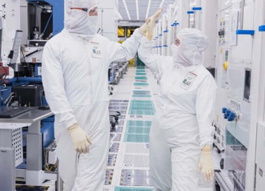
Our Manufacturing Technicians are critical to Intel and the future of technology. They are responsible for the setup, maintenance and performance of the complex machinery that build semiconductors—powering nearly everything in our daily lives. Whether you are right out of school, transitioning military, returning to the workforce or looking for a place that values your skills and expertise, we have a place for you at Intel.
-

Life at Intel
We've created an inclusive, supported environment...and we can't wait for you to be a part of it.
-

Learn More About the Semiconductor Industry
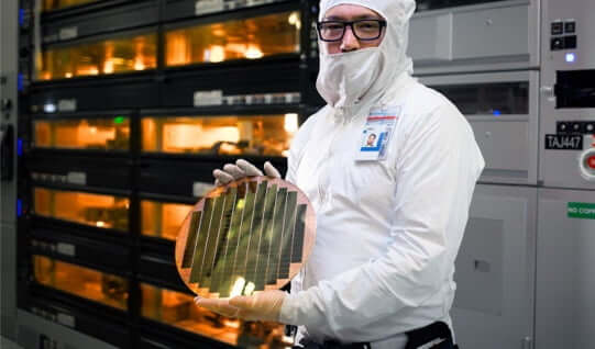
Semiconductors—otherwise known as microchips, microprocessors, or chips—are the brains behind some of the most innovative technology today and power so many of the things we use in our daily lives. There’s a big demand for them—and for the talented people who help bring this critical technology to life.
-

Intel to Receive Up to $8.5 Billion Through the CHIPS Act
Proposed funding, coupled with an investment tax credit and eligibility for CHIPS Act loans, would help Intel advance American semiconductor manufacturing and technology leadership in the AI era.
-

Intel Opens Fab 9 in New Mexico
Intel celebrated the opening of Fab 9, its cutting-edge factory in Rio Rancho, New Mexico. The milestone is part of Intel's previously announced $3.5 billion investment to equip its New Mexico operations for the manufacturing of advanced semiconductor packaging technologies.
-

The World’s First Systems Foundry
Intel launched Intel Foundry on February 21, 2024, as a more sustainable systems foundry business designed for the AI era. An expanded process roadmap was announced to establish leadership into the latter part of this decade.


