
Fab11x EMIB/FOVEROS Technology Product Integration Development Engineer
Job Description
Intel's Advanced Packaging (AP) technologies extend and drive Moore's Law as the company aspires to a trillion transistors in a package by 2030. Intel has led the industry in disaggregated advanced packaging for a couple of decades. Its innovations include EMIB (embedded multi-die interconnect bridge) and Foveros, technologies that allow multiple chips on a package to be connected side by side (EMIB) or stacked on top of one another in a 3D fashion (Foveros).
The Disaggregated Manufacturing Organization (DMO) develops fab processes for Foveros base silicon interposer and embedded multi-die interconnect silicon bride (EMIB) architectures to enable both internal and Foundry AP future roadmaps.
The New Mexico DMO Technology Development Team is looking for a Product Integration engineer to join our EMIB/FOVEROS TD team.
About the role:
EMIB/ FOVEROS TD Product Integration team coordinates and drives the TD team's test vehicle / early product roadmap and schedules, by working with layout/design, tapeout, mask manufacturing, fab, and post fab teams to ensure EMIB/ FOVEROS product requirements.
Yield Analysis Engineer responsibilities include but are not limited to:
- Working with fab team to define frame content to include on technology tape outs.
- Layout reviews to ensure designs are DRC and correct sizing applied before mask manufacture.
- Document product specific details, generate/audit/improve New Product/Technology Introduction checklists.
- Partner with TD team to ensure NPIs are intercepting expected process flow/recipes.
- Coordinate and own NPI scout lot setup/release/progress setting up flow.
- Develop strong partnerships with fab operations team to ensure critical NPI lots are meeting customer commitment.
The ideal candidate should exhibit the following behavioral traits:
- Understanding of post fab/pre-shipping wafer requirements
- Knowledge of NPI Checklist systems
- Preparing detailed, clear, and timely reports summarizing key lot status and driving organization to meet commitments.
- Basic understanding of the Interconnect process integration is a plus.
Relocation assistance provided.
Qualifications
You must possess the below minimum qualifications to be initially considered for this position. Preferred qualifications are in addition to the minimum requirements and are considered a plus factor in identifying top candidates. Experience listed below would be obtained through a combination of your schoolwork, classes, research and or relevant previous job and or internship experiences.
Minimum Qualifications:
- Bachelor's or Master's degree in Electrical Engineering, Physics, Material Science and Engineering, Computer Science, Chemical Engineering, Mechanical Engineering, Chemistry, or related field.
- This position is not eligible for Intel immigration sponsorship.
Preferred Qualifications:
- 1+ year(s) of experience with semiconductor processing fundamentals (lithography, wet and or dry etch, chemical and or mechanical polishing, etc.), semiconductor and or transistor device physics and design of experiments.
- 1+ year(s) of experience with materials characterization (SEM, TEM, etc.), materials fabrication, synthesis, or metrology
- 6+ months experience with model-based problem-solving technique to solve complex problems.
- Statistical data analysis (JMP, Excel, MATLAB, etc.)
- Demonstrated STEM research experience.
Inside this Business Group
As the world's largest chip manufacturer, Intel strives to make every facet of semiconductor manufacturing state-of-the-art -- from semiconductor process development and manufacturing, through yield improvement to packaging, final test and optimization, and world class Supply Chain and facilities support. Employees in the Technology Development and Manufacturing Group are part of a worldwide network of design, development, manufacturing, and assembly/test facilities, all focused on utilizing the power of Moore’s Law to bring smart, connected devices to every person on Earth.Posting Statement
All qualified applicants will receive consideration for employment without regard to race, color, religion, religious creed, sex, national origin, ancestry, age, physical or mental disability, medical condition, genetic information, military and veteran status, marital status, pregnancy, gender, gender expression, gender identity, sexual orientation, or any other characteristic protected by local law, regulation, or ordinance.Benefits
We offer a total compensation package that ranks among the best in the industry. It consists of competitive pay, stock, bonuses, as well as, benefit programs which include health, retirement, and vacation. Find more information about all of our Amazing Benefits here.Working Model
This role will be eligible for our hybrid work model which allows employees to split their time between working on-site at their assigned Intel site and off-site. In certain circumstances the work model may change to accommodate business needs.
Maggie Offensive Security Researcher
Saya sentiasa mahu melakukan sesuatu yang mengubah dunia — di Intel, saya rasa dihargai, dan saya semakin yakin pada diri saya sendiri. Ia membuatkan saya berasa seperti saya mampu melakukan perkara yang hebat.
- IP Design Micro-Architect / Lead Malaysia Mohon sekarang
- PCIe Design Verification Lead Engineer Berbilang Lokasi Mohon sekarang
- Senior SoC SDM Architect Berbilang Lokasi Mohon sekarang
Anda belum mempunyai Kerja Disimpan lagi.
Lihat Semua PekerjaanSpotlight
-

-
-
-
-
-
Our Hiring Process
See all the steps of the recruitment process at Intel – from apply to interview.
-
Faedah
Terdapat banyak cuti berbayar, pilihan saham, pendidikan berterusan, bonus dan lain-lain lagi. Ia merangkumi semua yang anda perlukan untuk berkembang maju.
-
Pelatih dan Graduan Baru
Bersedia untuk memulakan lebih daripada sekadar kerjaya anda? Ini boleh menjadi titik permulaan sesuatu yang luar biasa.
-
Kehidupan di Intel
Kami telah mencipta persekitaran yang inklusif dan disokong dan kami tidak sabar untuk anda menjadi sebahagian daripadanya.
-
Our Software Teams
Intel is one of the largest and most influential software companies in the world. See software jobs for developers and engineers at Intel.
-
-
Our Graphics Teams
Drive innovation in graphics for media streaming, gaming, AI, and more. See GPU, embedded graphics, and graphics software engineering jobs at Intel.
-


Sertai komuniti bakat kami
Jadilah orang pertama untuk mendapatkan berita perkembangan terkini di Intel! Daftar untuk menerima berita terkini.
-
Manufacturing at Intel
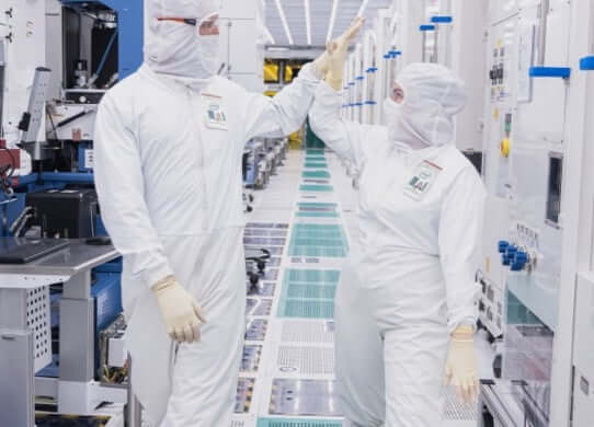
Our Manufacturing Technicians are critical to Intel and the future of technology. They are responsible for the setup, maintenance and performance of the complex machinery that build semiconductors—powering nearly everything in our daily lives. Whether you are right out of school, transitioning military, returning to the workforce or looking for a place that values your skills and expertise, we have a place for you at Intel.
-

Life at Intel
We've created an inclusive, supported environment...and we can't wait for you to be a part of it.
-

Learn More About the Semiconductor Industry
Semiconductors—otherwise known as microchips, microprocessors, or chips—are the brains behind some of the most innovative technology today and power so many of the things we use in our daily lives. There’s a big demand for them—and for the talented people who help bring this critical technology to life.
-

Intel to Receive Up to $8.5 Billion Through the CHIPS Act
Proposed funding, coupled with an investment tax credit and eligibility for CHIPS Act loans, would help Intel advance American semiconductor manufacturing and technology leadership in the AI era.
-

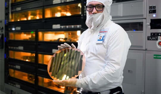
Intel Opens Fab 9 in New Mexico
Intel celebrated the opening of Fab 9, its cutting-edge factory in Rio Rancho, New Mexico. The milestone is part of Intel's previously announced $3.5 billion investment to equip its New Mexico operations for the manufacturing of advanced semiconductor packaging technologies.
-
The World’s First Systems Foundry
Intel launched Intel Foundry on February 21, 2024, as a more sustainable systems foundry business designed for the AI era. An expanded process roadmap was announced to establish leadership into the latter part of this decade.


