
Ocotillo Technology Fabrication Yield Module Engineering Graduate Intern
Job Description
OTF (Ocotillo Technology Fabrication) is looking for highly motivated individuals with a strong technical background to play a key role in the continuous improvement of leading-edge semiconductor manufacturing processes. Selected individuals will work in the OTF Yield department and drive improvements in quality, yield, defectivity, reliability, cost, process stability/capability, electrical performance and productivity through data analysis and application of engineering knowledge. The role will include both team-based work, as well as self-driven individual projects.
This OTF's Yield Engineering Internship positions is a Year-Round, on-campus opportunity. Interns who will work part time (15-31 hours/week) during the school year and full time (40 hours/week) in the summer, onsite at the Ocotillo Campus. Hybrid/virtual work schedules are not permitted. Candidates will not work more than 31 hours during the school semester. Ideally, candidates must be able to start this position on September 3rd.
Job responsibilities may include, but are not limited to:
- Partnering with a team of engineers to design experiments aimed at continuous improvement activities, which range from yield enhancement, defect reduction, cost reduction, and productivity / output improvement
- Performing detailed data analysis using various statistical/data mining tools to identify the root cause of defect/yield/quality issues
- Identifying exclusionary or baseline sources of defects and recommending/leading corrective actions/fixes.
- Creating quality systems to simultaneously increase productivity and quality output
- Ensure the manufacturing process is producing transistor and discrete electronic devices that perform according to strictly defined specifications
- Upskill peers on their areas of expertise through sharing forums
- Engage in creative problem-solving skills and lateral thinking (the solving of problems by an indirect and creative approach, typically through viewing the problem in a new and unusual light) desired to help deal with the high level of ambiguity that is associated with the problems often encountered in the job role.
The ideal candidate should exhibit the following behavioral traits:
- Solid analytical skills and a passion for data analysis and problem solving.
- Strong organizational skills with an attention to detail.
- Excellent communication and presentation skills to influence a wide variety of groups at all levels
- High level of personal integrity with a positive attitude
- Willingness to contribute to a team, or take the lead as needed
Qualifications
Minimum qualifications are required to be initially considered for this position. Preferred qualifications are in addition to the minimum requirements and are considered a plus factor in identifying top candidates.
Minimum Qualifications:
- Must be an actively enrolled and progressing as a student pursuing a Masters of science or Doctoral degree in Chemical Engineering, Electrical Engineering, Material Science, Microelectronics Engineering, Optical Engineering, Physics or related field.
- Must possess and maintain a minimum GPA of 3.0 for the duration of the internship.
- Must maintain full-time student status during internship (minimum 12 credit hours /semester).
Preferred Qualifications:
- Statistical Data Analysis. Examples include: JMP/JSL, Python, Machine Learning.
- Knowledge of Design of Experiment DOE principles.
- Statistical Process Control SPC Theory.
- Physics of Semiconductor Materials.
- Semiconductor fabrication and processing techniques Lithography, Etch, CMP, Thin Films, Plating, etc.
- Materials Analysis techniques such as SEM, TEM, EDX, SIMS, XPS, XRD, FTIR or Auger.
- Programing Experience: Preferred languages include, but are not limited to: Python, C#, JSL.
This position is in Chandler, Arizona at Intel's Ocotillo Facility. Relocation assistance will not be provided.
Inside this Business Group
As the world's largest chip manufacturer, Intel strives to make every facet of semiconductor manufacturing state-of-the-art -- from semiconductor process development and manufacturing, through yield improvement to packaging, final test and optimization, and world class Supply Chain and facilities support. Employees in the Technology Development and Manufacturing Group are part of a worldwide network of design, development, manufacturing, and assembly/test facilities, all focused on utilizing the power of Moore’s Law to bring smart, connected devices to every person on Earth.Posting Statement
All qualified applicants will receive consideration for employment without regard to race, color, religion, religious creed, sex, national origin, ancestry, age, physical or mental disability, medical condition, genetic information, military and veteran status, marital status, pregnancy, gender, gender expression, gender identity, sexual orientation, or any other characteristic protected by local law, regulation, or ordinance.Benefits
We offer a total compensation package that ranks among the best in the industry. It consists of competitive pay, stock, bonuses, as well as, benefit programs which include health, retirement, and vacation. Find more information about all of our Amazing Benefits here.Annual Salary Range for jobs which could be performed in the US $63,000.00-$166,000.00 (Hourly Role)
*Salary range dependent on a number of factors including location and experience
Working Model
This role will require an on-site presence.* Job posting details (such as work model, location or time type) are subject to change...
Maggie 前沿安全研究員
“我一直夢想改變世界。在英特爾,我能發揮長,並且更有自信。因此,我放眼完成壯舉。”
Spotlight
-

-
-
-
福利
我們提供讓您茁壯成長所需的一切條件,包括豐富的有薪假期、股票計劃、進修機會、工作獎金等等
-
實習生和應屆畢業生
準備好啟動你與眾不同的職業生涯了嗎?這裡也許是你非凡旅途的開始。
-
英特爾工作文化
我們為你打造一流的工作環境,歡迎加入我們的行列。
-
-
Our Hiring Process
See all the steps of the recruitment process at Intel – from apply to interview.
-
Our Software Teams
Intel is one of the largest and most influential software companies in the world. See software jobs for developers and engineers at Intel.
-
-
Our Graphics Teams
Drive innovation in graphics for media streaming, gaming, AI, and more. See GPU, embedded graphics, and graphics software engineering jobs at Intel.
-


加入人才社區
隨時留意英特爾的最新動態!註冊訂閱我們的最新消息和更新。
-
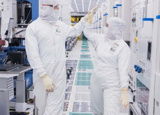
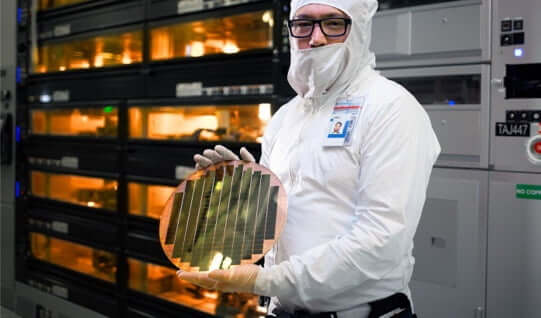
Manufacturing at Intel
Our Manufacturing Technicians are critical to Intel and the future of technology. They are responsible for the setup, maintenance and performance of the complex machinery that build semiconductors—powering nearly everything in our daily lives. Whether you are right out of school, transitioning military, returning to the workforce or looking for a place that values your skills and expertise, we have a place for you at Intel.
-

Life at Intel
We've created an inclusive, supported environment...and we can't wait for you to be a part of it.
-

Learn More About the Semiconductor Industry
Semiconductors—otherwise known as microchips, microprocessors, or chips—are the brains behind some of the most innovative technology today and power so many of the things we use in our daily lives. There’s a big demand for them—and for the talented people who help bring this critical technology to life.
-

Intel to Receive Up to $8.5 Billion Through the CHIPS Act
Proposed funding, coupled with an investment tax credit and eligibility for CHIPS Act loans, would help Intel advance American semiconductor manufacturing and technology leadership in the AI era.
-

Intel Opens Fab 9 in New Mexico
Intel celebrated the opening of Fab 9, its cutting-edge factory in Rio Rancho, New Mexico. The milestone is part of Intel's previously announced $3.5 billion investment to equip its New Mexico operations for the manufacturing of advanced semiconductor packaging technologies.
-
The World’s First Systems Foundry
Intel launched Intel Foundry on February 21, 2024, as a more sustainable systems foundry business designed for the AI era. An expanded process roadmap was announced to establish leadership into the latter part of this decade.


