
FSM Senior Device Integration Engineer - Foundry
Job Description
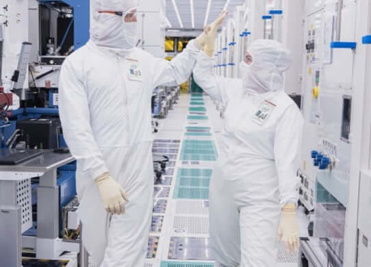
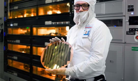
Fab Sort Manufacturing (FSM) is responsible for the production of all Intel silicon using some of the world's most advanced manufacturing processes in fabs in Arizona, Ireland, Israel, Oregon and 2 new greenfield sites in Ohio and Germany. As part of Intel's strategy, FSM is rapidly expanding its operation to deliver output for both internal and foundry customers with state-of-the-art technologies arriving in High-Volume Manufacturing (HVM) at a 2-year cadence going forward.
Intel recently created the HVM Global Yield organization in FSM to strengthen its yield operation and enable fast-paced yield ramp-up in early HVM phases for each technology in collaboration with Technology Development team and FSM fab managers.
This position is for a Senior Engineer in the Device Integration team in the FSM HVM Global Yield organization, reporting to the Manager/Director of Device Integration Engineering. The selected candidate will work with other members in Global Yield org including Process Integration, Yield Analysis and Defect engineering teams, fab module/yield teams and TD team members to achieve yield ramp-up and process optimization in early production stage, supporting internal and external customers.
The Device Integration engineer's responsibilities include (but are not limited to):
- Own engineering projects to execute HVM yield roadmap, device targeting and attain performance targets.
- Collaborate with Technology Development team to develop new device technology, customize device architecture per customer request and import to production fabs.
- Participate or lead cross-organizational team of engineers to identify root cause of device-related yield/performance issues and define mitigation plan to meet committed production yield/performance targets.
- Own NPI (New Product Introduction) in production fabs and perform device-related process optimization to meet foundry customers product specifications and requirements.
- Develop a model to predict device performance accurately in early-to-mid stage of Si progression and drive systematic solution to maintain baseline device performance.
- Work with Process Integration engineers to drive process simplification and implement cost reduction engineering opportunities in line.
#foundry
Important: Please be informed that Intel is proactively trying to find candidates for a foundry engineering position which is frequently available at Intel US. Please note that the position may not be available at this time. If you would be interested in this position should it become available, we would encourage you to apply, and our hiring team will be glad to contact you when/if relevant.
Qualifications
Minimum Qualifications:
- Bachelor's degree in Electrical Engineering, Physics or Materials Science major. Other related science and engineering degrees can be considered based on industry experience.
- 6+ years' experience in advanced node semiconductor industry in Device Integration.
- Experience in FinFET technology development or high-volume manufacturing.
- Experience with Device Physics and hands-on application in real-world fab environment.
- Experience with FEOL (Front-End-Of-Line) Integration teams including Fin, Poly, Source-Drain and Gate segments on Device performance improvement and targeting with technical understanding on how FEOL process changes impact Device parameters.
Preferred Qualifications:
- Advanced degree (Master's or Ph.D.) in Electrical Engineering, Physics or Materials Science major.
- Experience in project/program management and/or Task Force Team lead.
- Demonstrated interpersonal skills including influencing, engaging, and motivating.
- Experience in serving external Foundry customers through technical interactions.
- Experience in GAA (Gate-All-Around) technology architecture.
- Experience in new semiconductor technology development.
- Basic understanding and collaboration experience with module processes including lithography, dry etch, wet etch, CMP, diffusion, implant, thin films and metrology.
Posting Statement
All qualified applicants will receive consideration for employment without regard to race, color, religion, religious creed, sex, national origin, ancestry, age, physical or mental disability, medical condition, genetic information, military and veteran status, marital status, pregnancy, gender, gender expression, gender identity, sexual orientation, or any other characteristic protected by local law, regulation, or ordinance.Benefits
We offer a total compensation package that ranks among the best in the industry. It consists of competitive pay, stock, bonuses, as well as, benefit programs which include health, retirement, and vacation. Find more information about all of our Amazing Benefits here.Working Model
This role will be eligible for our hybrid work model which allows employees to split their time between working on-site at their assigned Intel site and off-site. In certain circumstances the work model may change to accommodate business needs.
Maggie 前沿安全研究員
“我一直夢想改變世界。在英特爾,我能發揮長,並且更有自信。因此,我放眼完成壯舉。”
Spotlight
-

-
-
-
-
Our Hiring Process
See all the steps of the recruitment process at Intel – from apply to interview.
-
福利
我們提供讓您茁壯成長所需的一切條件,包括豐富的有薪假期、股票計劃、進修機會、工作獎金等等
-
實習生和應屆畢業生
準備好啟動你與眾不同的職業生涯了嗎?這裡也許是你非凡旅途的開始。
-
英特爾工作文化
我們為你打造一流的工作環境,歡迎加入我們的行列。
-
Our Software Teams
Intel is one of the largest and most influential software companies in the world. See software jobs for developers and engineers at Intel.
-


加入人才社區
隨時留意英特爾的最新動態!註冊訂閱我們的最新消息和更新。
-
Manufacturing at Intel
Our Manufacturing Technicians are critical to Intel and the future of technology. They are responsible for the setup, maintenance and performance of the complex machinery that build semiconductors—powering nearly everything in our daily lives. Whether you are right out of school, transitioning military, returning to the workforce or looking for a place that values your skills and expertise, we have a place for you at Intel.
-

Life at Intel
We've created an inclusive, supported environment...and we can't wait for you to be a part of it.
-

Learn More About the Semiconductor Industry
Semiconductors—otherwise known as microchips, microprocessors, or chips—are the brains behind some of the most innovative technology today and power so many of the things we use in our daily lives. There’s a big demand for them—and for the talented people who help bring this critical technology to life.
-

Intel to Receive Up to $8.5 Billion Through the CHIPS Act
Proposed funding, coupled with an investment tax credit and eligibility for CHIPS Act loans, would help Intel advance American semiconductor manufacturing and technology leadership in the AI era.
-

Intel Opens Fab 9 in New Mexico
Intel celebrated the opening of Fab 9, its cutting-edge factory in Rio Rancho, New Mexico. The milestone is part of Intel's previously announced $3.5 billion investment to equip its New Mexico operations for the manufacturing of advanced semiconductor packaging technologies.
-
The World’s First Systems Foundry
Intel launched Intel Foundry on February 21, 2024, as a more sustainable systems foundry business designed for the AI era. An expanded process roadmap was announced to establish leadership into the latter part of this decade.


