Transmission Electron Microscopy (TEM) Engineer
Job Description
Fab Sort Manufacturing (FSM) is responsible for the production of all Intel silicon using some of the world's most advanced manufacturing processes in fabs in Arizona, Ireland, Israel, Oregon and 2 new greenfield sites in Ohio and Germany.
Intel recently created HVM Global Yield organization in FSM to strengthen its yield operation and enable fast-paced yield ramp-up in early HVM phases for each technology in collaboration with Technology Development (TD) team, and FSM fab managers.
This job requisition is seeking a Transmission Electron Microscopy (TEM) Engineer working in our FSM Ireland Analytical Laboratories which operate 24/7. Selected candidate will work in a dynamic team supporting technology development & yield improvement. The TEM group uses the latest state-of-the-art workflows leveraging a high level of autonomy. TEM engineers may support conventional manual TEM or oversee engineering for autonomous lines. This requisition has multiple openings on both night and day shifts.
TEM Engineers responsibilities include (but are not limited to):
Review incoming requests and determining appropriate TEM workflow strategy. Prepare plans as appropriate for TEM sample preparation team.
Hands on operation of laboratory equipment, such as TEM microscopes.
Monitoring & oversight of autonomous TEM sample production line, ensuring maximum uptime and sample throughput.
Interpretation of complex TEM results, translating to actionable data for FAB process and integration teams.
Support continual improvement & development of new workstreams & techniques.
Develop a thorough understanding of manual and autonomous TEM operation lines.
Mentor junior TEM engineers & TEM preparation technicians.
Candidate should have the following behavioral skills:
Demonstrated strength in teamwork, analytical problem solving, and effective oral and written communication skills.
Inquisitive, desire to learn and expand knowledge in field.
Ability to work with multi-functional, multi-cultural teams.
Strong in decision making and problem solving.
Qualifications
Minimum Qualifications:
Master’s degree in science and engineering major.
Greater than 2 years’ experience in a TEM engineering laboratory.
Preferred Qualifications:
Ph.D. in science and engineering major.
Greater than 5 years’ experience operating a Transmission Electron Microscope and material characterization techniques.
Experience with various types of TEM sample preparation.
Strong TEM interpretation skillset
Understanding of FinFET technology architecture.
Knowledge of wafer fabrication and general microelectronics.
Willingness to work night shift.
Posting Statement
All qualified applicants will receive consideration for employment without regard to race, color, religion, religious creed, sex, national origin, ancestry, age, physical or mental disability, medical condition, genetic information, military and veteran status, marital status, pregnancy, gender, gender expression, gender identity, sexual orientation, or any other characteristic protected by local law, regulation, or ordinance.Benefits
We offer a total compensation package that ranks among the best in the industry. It consists of competitive pay, stock, bonuses, as well as, benefit programs which include health, retirement, and vacation. Find more information about all of our Amazing Benefits here.
Maggie Offensive Security Researcher
Tôi luôn muốn đóng góp được điều gì đó giúp thay đổi thế giới. Tại Intel, tôi cảm thấy mình được đánh giá cao và tự tin hơn vào bản thân. Điều đó khiến tôi nghĩ rằng mình có khả năng làm được những điều tuyệt vời.
- ESD Design Engineer San José, Cốt-xta Ri-ca Ứng tuyển ngay
- Product Development Engineer - High Volume San José, Cốt-xta Ri-ca Ứng tuyển ngay
- Product Development Engineer - High Volume San José, Cốt-xta Ri-ca Ứng tuyển ngay
Bạn chưa có công việc đã lưu.
Xem toàn bộ công việcTham gia vào cộng đồng nhân tài của Intel
Hãy là người đầu tiên cập nhật mọi tin tức từ Intel! Đăng ký để nhận những tin tức và thông báo mới nhất.
-

Manufacturing at Intel
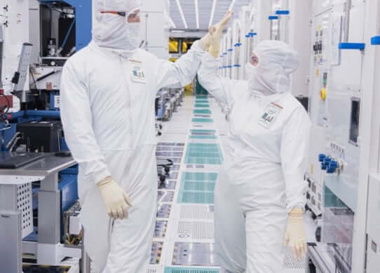
Our Manufacturing Technicians are critical to Intel and the future of technology. They are responsible for the setup, maintenance and performance of the complex machinery that build semiconductors—powering nearly everything in our daily lives. Whether you are right out of school, transitioning military, returning to the workforce or looking for a place that values your skills and expertise, we have a place for you at Intel.
-

Life at Intel
We've created an inclusive, supported environment...and we can't wait for you to be a part of it.
-

Learn More About the Semiconductor Industry
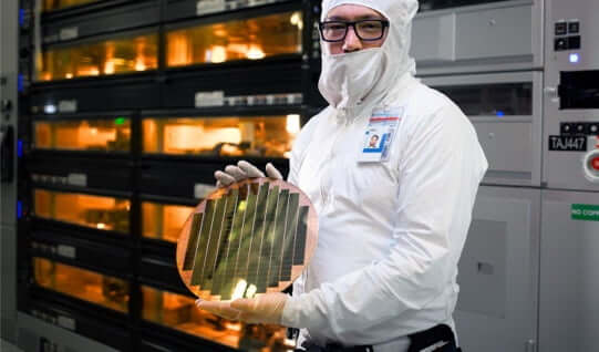
Semiconductors—otherwise known as microchips, microprocessors, or chips—are the brains behind some of the most innovative technology today and power so many of the things we use in our daily lives. There’s a big demand for them—and for the talented people who help bring this critical technology to life.
-

Intel to Receive Up to $8.5 Billion Through the CHIPS Act
Proposed funding, coupled with an investment tax credit and eligibility for CHIPS Act loans, would help Intel advance American semiconductor manufacturing and technology leadership in the AI era.
-

Intel Opens Fab 9 in New Mexico
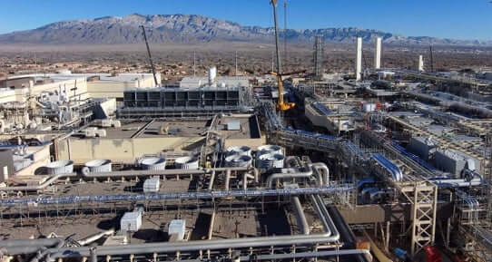
Intel celebrated the opening of Fab 9, its cutting-edge factory in Rio Rancho, New Mexico. The milestone is part of Intel's previously announced $3.5 billion investment to equip its New Mexico operations for the manufacturing of advanced semiconductor packaging technologies.
-

The World’s First Systems Foundry
Intel launched Intel Foundry on February 21, 2024, as a more sustainable systems foundry business designed for the AI era. An expanded process roadmap was announced to establish leadership into the latter part of this decade.


