
Sr. Device Characterization Engineer
Job Description
Fab Sort Manufacturing (FSM) is responsible for the production of all Intel silicon using some of the world's most advanced manufacturing processes in fabs in Arizona, Ireland, Israel, Oregon and a new greenfield site in Ohio.Intel recently created the Global Yield organization in FSM to strengthen its yield operation and enable fast-paced yield ramp-up in early HVM phases for each technology in collaboration with Technology Development (TD) team, and FSM fabs.This job requisition is seeking a Sr. Device Characterization Engineer to startup and lead the device characterization operation within the Global Yield Development Lab's Arizona location. Selected expert will lead our offline engineering device characterization lab, developing and executing advanced characterization plans and providing general device troubleshooting support. This high visibility role is a key enabler for device development and process optimization in early production stage for our global development network.Sr. Device Characterization Engineer's responsibilities include (but are not limited to):
- Development and execution of characterization and testing plans to extract required electrical information.
- Conduct higher level investigation and evaluation of devices, including initial device model generation along with providing insight to customers on key observations and possible reasons.
- Provide technical guidance and mentorship to junior device engineers and technicians, fostering a strong culture of continuous learning and development.
- Maintain safe and professional device characterization laboratory, providing data of the highest integrity and role modeling best practices for equipment calibration.
- Candidate should have the following behavioral skills:
- Demonstrated strength in leadership, teamwork, problem solving, and effective oral and written communication skills.
- Ability to work with multi-functional, multi-cultural teams.
- Strong decision making and problem-solving ability.
- A good motivator, with ability to listen.
Qualifications
Minimum qualifications are required to be initially considered for this position. Preferred qualifications are in addition to the minimum requirements and are considered a plus factor in identifying top candidates.Minimum Qualifications:
- Advanced degree (Master's or Ph.D.) in physics, electronic engineering or science related major with 3+ years' device characterization experience
- Demonstrated expertise in CMOS semiconductor device physics and advanced transistor device architectures.
- Proficiency in the generation and analysis of device parametric data and implementation of scripting and engineering data analysis routines.
- Hands on experience setting up and conducting manual and semi-automated wafer level device characterization.
- Self-sufficient with a broad knowledge of electrical measurement techniques such as I-V/C-V measurements.
- Proficiency in excel and scripting including Python and LabVIEW.
Preferred Qualifications
- Inquisitiveness and self-driven; can quickly become an expert on a semiconductor device architecture, function and assess performance.
- Significant knowledge of Formfactor CM300 probers along with operation of electrical test equipment such as Keysight B1500 parametric analyzers, Keithley switches, and LCR's.
- Probe card design and drawing interpretation.
- Experience with management and oversight of a device characterization lab.
- Experience with compact modeling and device simulation.
Requirements listed would be obtained through a combination of industry relevant job experience, internship experiences and or schoolwork/classes/research.
Inside this Business Group
As the world's largest chip manufacturer, Intel strives to make every facet of semiconductor manufacturing state-of-the-art -- from semiconductor process development and manufacturing, through yield improvement to packaging, final test and optimization, and world class Supply Chain and facilities support. Employees in the Technology Development and Manufacturing Group are part of a worldwide network of design, development, manufacturing, and assembly/test facilities, all focused on utilizing the power of Moore’s Law to bring smart, connected devices to every person on Earth.Posting Statement
All qualified applicants will receive consideration for employment without regard to race, color, religion, religious creed, sex, national origin, ancestry, age, physical or mental disability, medical condition, genetic information, military and veteran status, marital status, pregnancy, gender, gender expression, gender identity, sexual orientation, or any other characteristic protected by local law, regulation, or ordinance.Benefits
We offer a total compensation package that ranks among the best in the industry. It consists of competitive pay, stock, bonuses, as well as, benefit programs which include health, retirement, and vacation. Find more information about all of our Amazing Benefits here.Annual Salary Range for jobs which could be performed in the US $153,100.00-$216,140.00*Salary range dependent on a number of factors including location and experienceWorking Model
This role will be eligible for our hybrid work model which allows employees to split their time between working on-site at their assigned Intel site and off-site. * Job posting details (such as work model, location or time type) are subject to change.
Maggie 前沿安全研究員
“我一直夢想改變世界。在英特爾,我能發揮長,並且更有自信。因此,我放眼完成壯舉。”
Spotlight


Join Our Job Alerts
Let’s stay connected. Sign up to receive alerts when new opportunities become available that match your career ambitions.
加入人才社區
隨時留意英特爾的最新動態!註冊訂閱我們的最新消息和更新。
-
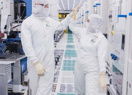
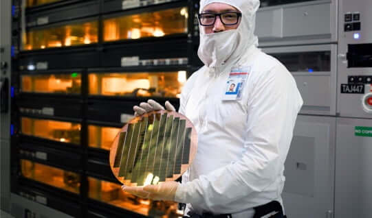
Manufacturing at Intel
Our Manufacturing Technicians are critical to Intel and the future of technology. They are responsible for the setup, maintenance and performance of the complex machinery that build semiconductors—powering nearly everything in our daily lives. Whether you are right out of school, transitioning military, returning to the workforce or looking for a place that values your skills and expertise, we have a place for you at Intel.
-

Life at Intel
We can't wait for you to be part of our team.
-

Learn more About the Semiconductor Industry
Semiconductors—otherwise known as microchips, microprocessors, or chips—are the brains behind some of the most innovative technology today and power so many of the things we use in our daily lives. There’s a big demand for them—and for the talented people who help bring this critical technology to life.
-
Intel to Receive Up to $8.5 Billion Through the CHIPS Act
Proposed funding, coupled with an investment tax credit and eligibility for CHIPS Act loans, would help Intel advance American semiconductor manufacturing and technology leadership in the AI era.
-

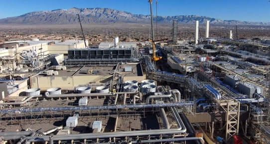
Intel Opens Fab 9 in New Mexico
Intel celebrated the opening of Fab 9, its cutting-edge factory in Rio Rancho, New Mexico. The milestone is part of Intel's previously announced $3.5 billion investment to equip its New Mexico operations for the manufacturing of advanced semiconductor packaging technologies.
-
The World’s First Systems Foundry
Intel launched Intel Foundry on February 21, 2024, as a more sustainable systems foundry business designed for the AI era. An expanded process roadmap was announced to establish leadership into the latter part of this decade.


