
Global Yield BEOL Senior Process Integration Development Engineer
Job Description
Join Global Yield and experience the exciting transition of Intel technology development from Oregon to Intel High Volume Manufacturing Fabs.Global Yield is part of Fab Sort Manufacturing (FSM).
FSM is responsible for the production of Intel silicon using the world's most advanced manufacturing processes in fabs in Europe and Ireland.
As a key deliverable for IDM2.0 strategy, Global Yield was formed to drive continuous process technology development within FSM; in support of yield improvement, MOR changes, and Foundry Customer optimizations.
This job requisition is to seek BEOL (Back-End-Of-Line) Process Integration engineering roles in FSM HVM Global Yield organization, reporting to BEOL Process Integration manager.
Selected candidates will work with other members in BEOL integration, other teams in Global Yield org, fab module, yield, and TD team members to achieve yield ramp-up and process optimization in early production stage, supporting internal and external customers.
Responsibilities will include but are not limited to:
Provides sustaining support of module equipment/ module components and supports installation and qualification of new module equipment/ module components.
Own engineering projects to execute HVM yield roadmap, device targeting, focusing on Cu BEOL integration.
Collaborate with BEOL Technology Development team to import new technology to production fabs.
Work with FEOL/BEOL Integration, Device, Defect Reduction and Yield Analysis team members to identify root cause of yield/performance issues and implement mitigation plan in defined timeline to meet committed production yield/performance targets and to support fast paced yield ramp-up in high-volume manufacturing phases.
Own engineering projects to improve product yield, quality, performance and to reduce wafer cost.
Engineering support for technical interactions with internal and external customers.
Candidate should possess the following behavioral skills:
Problem-solving technique with self-initiative and self-learning capabilities.
Comfortable working with a high degree of autonomy.
Capacity to work with multi-functional, multi-cultural teams.
Communication skills.
Qualifications
You must possess the below minimum qualifications to be initially considered for this position. Preferred qualifications are in addition to the minimum requirements and are considered a plus factor in identifying top candidates.Minimum Qualifications:
- Bachelor's Degree in Electrical Engineering, Physics, Chemistry, Materials Science or in a STEM related Field.
- 9+ years of experience in advanced node semiconductor industry in BEOL Process Integration.
- 9+ years of experience with Device Physics and backend critical parameter control.
- 9+ years of experience with processes including lithography, dry etch, wet etch, CMP, diffusion, implant, thin films and metrology.
Preferred Qualifications:Experience in SADP/SAQP, advanced metallization, and/or immersion lithography/EUV).Advanced (Masters or PhD) degree in Electrical Engineering, Physics, Chemistry, Materials Science or in a STEM related Field.Experience in project/program management and/or Task Force Team lead.Experience in leveraging big data analysis to identify process design weaknesses and/or manufacturing weaknesses in order to propose corrective, data-based solutions.Experience with extracting insights from structured and unstructured data by quickly synthesizing large volumes of data and applying statistics and machine learning.Experience in new semiconductor technology development.Experience in serving external Foundry customers through technical interactions.Experience in latest lithography and metallization device architectures.Experience in Statistics and machine learning preferred.Previous related work experience in a semiconductor foundry preferred
Inside this Business Group
As the world's largest chip manufacturer, Intel strives to make every facet of semiconductor manufacturing state-of-the-art -- from semiconductor process development and manufacturing, through yield improvement to packaging, final test and optimization, and world class Supply Chain and facilities support. Employees in the Technology Development and Manufacturing Group are part of a worldwide network of design, development, manufacturing, and assembly/test facilities, all focused on utilizing the power of Moore’s Law to bring smart, connected devices to every person on Earth.Posting Statement
All qualified applicants will receive consideration for employment without regard to race, color, religion, religious creed, sex, national origin, ancestry, age, physical or mental disability, medical condition, genetic information, military and veteran status, marital status, pregnancy, gender, gender expression, gender identity, sexual orientation, or any other characteristic protected by local law, regulation, or ordinance.Benefits
We offer a total compensation package that ranks among the best in the industry. It consists of competitive pay, stock, bonuses, as well as, benefit programs which include health, retirement, and vacation. Find more information about all of our Amazing Benefits here.Annual Salary Range for jobs which could be performed in the US $179,900.00-$253,980.00*Salary range dependent on a number of factors including location and experienceWorking Model
This role will be eligible for our hybrid work model which allows employees to split their time between working on-site at their assigned Intel site and off-site. * Job posting details (such as work model, location or time type) are subject to change.
Maggie Offensive Security Researcher
Saya sentiasa mahu melakukan sesuatu yang mengubah dunia — di Intel, saya rasa dihargai, dan saya semakin yakin pada diri saya sendiri. Ia membuatkan saya berasa seperti saya mampu melakukan perkara yang hebat.
Anda belum mempunyai Kerja Disimpan lagi.
Lihat Semua PekerjaanSpotlight
-

Kehidupan di Intel
Kami telah mencipta persekitaran yang inklusif dan disokong dan kami tidak sabar untuk anda menjadi sebahagian daripadanya.
-

Faedah
Terdapat banyak cuti berbayar, pilihan saham, pendidikan berterusan, bonus dan lain-lain lagi. Ia merangkumi semua yang anda perlukan untuk berkembang maju.
-

Pelatih dan Graduan Baru
Bersedia untuk memulakan lebih daripada sekadar kerjaya anda? Ini boleh menjadi titik permulaan sesuatu yang luar biasa.
Join Our Job Alerts
Let’s stay connected. Sign up to receive alerts when new opportunities become available that match your career ambitions.
Sertai komuniti bakat kami
Jadilah orang pertama untuk mendapatkan berita perkembangan terkini di Intel! Daftar untuk menerima berita terkini.
-
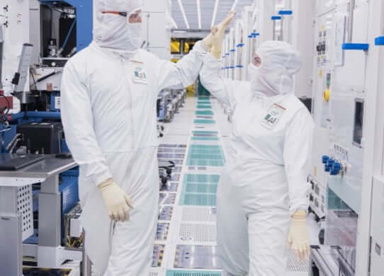
Manufacturing at Intel
Our Manufacturing Technicians are critical to Intel and the future of technology. They are responsible for the setup, maintenance and performance of the complex machinery that build semiconductors—powering nearly everything in our daily lives. Whether you are right out of school, transitioning military, returning to the workforce or looking for a place that values your skills and expertise, we have a place for you at Intel.
-

Life at Intel
We can't wait for you to be part of our team.
-

Learn more About the Semiconductor Industry
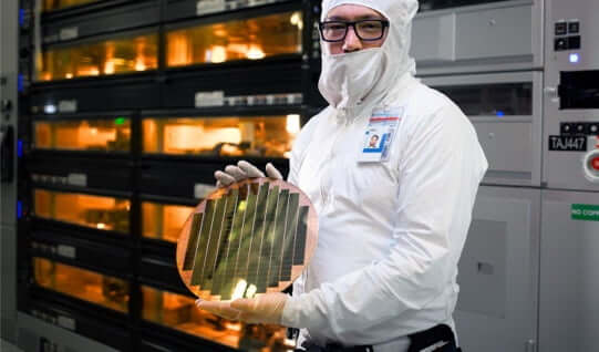
Semiconductors—otherwise known as microchips, microprocessors, or chips—are the brains behind some of the most innovative technology today and power so many of the things we use in our daily lives. There’s a big demand for them—and for the talented people who help bring this critical technology to life.
-
Intel to Receive Up to $8.5 Billion Through the CHIPS Act
Proposed funding, coupled with an investment tax credit and eligibility for CHIPS Act loans, would help Intel advance American semiconductor manufacturing and technology leadership in the AI era.
-

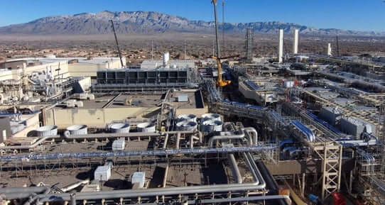
Intel Opens Fab 9 in New Mexico
Intel celebrated the opening of Fab 9, its cutting-edge factory in Rio Rancho, New Mexico. The milestone is part of Intel's previously announced $3.5 billion investment to equip its New Mexico operations for the manufacturing of advanced semiconductor packaging technologies.
-
The World’s First Systems Foundry
Intel launched Intel Foundry on February 21, 2024, as a more sustainable systems foundry business designed for the AI era. An expanded process roadmap was announced to establish leadership into the latter part of this decade.


